* Precision cold forging method of complex shape
* Precision shearing technique
* Forming technique by using hard-to-process metals
* Technique of mirror-finished inner surface
* Joint study of prototype products and development articles
* Prediction and verification analyzed by CAE
* Cost reduction as a result of changing mechanical processing method
* Materials analysis and measurement at a nano level
* Development of new materials
* Material strength test
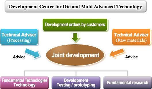
Our specialists quickly respond to any requests of a development project, a test production or a collaborative research from our customer.
We respond to our customer's various needs by applying our advanced technology which we worked with our specialists from university laboratories to develop.
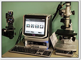
Measuring machine
We line up most advanced high-precision measuring machines, i.e. electron microscope, CMM, CNC, 3D Optical Surface Profiler etc., to handle various measurements.
We promise we will offer you high-quality products based on our quality control system.
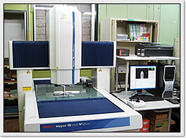
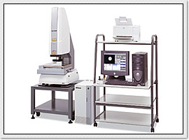
High functionality CNC Vision Measuring System
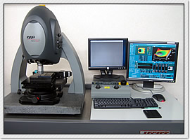
3D Optical Surface Profiler (ZYGO)
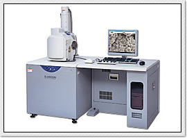
Scanning Electron Microscope (SEM)
High-speed Microscope
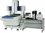
CNC Video Measuring System (Nikon: Nexiv)
Point Autofocus Probe Surface Texture Measuring Instrument
High functionality CNC Vision Measuring System
Model
QV-HYPER606 (Mitsutoyo)
Minimum display unit
0.02μm
Measuring range
600×650×250
Measurement accuracy
X and Y axes (0.8+2L/1000) μm
Z axis (1.5+2L/1000) μm
X plane (1.4+3L/1000) μm
Standard equipment: RGB color LED illumination, Programmable Power Turret (PPT), Programmable Ring Light (PRL).
A low-thermal expansion stage glass (linear expansion coefficient (0±0.02) × 10-6/K) helps to minimize errors by temparatures.
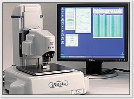
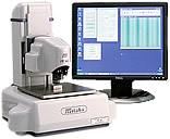
Point Autofocus Probe Surface Texture Measuring Instrument
Model
PF-60 (Mitaka)
Measuring range
60×60×10
Optical resolution
XY=0.1μm Z=0.01μm
Measurement accuracy
X axes (2 + 4L/1000) μm
Y axes (2 + 4L/1000) μm
Z axes (0.3 + 0.5L/10) μm
Scan AF and high precision XY scanning stage enables to measure a wide range of tens of mm with sub-micron accuracy.
PF-60 enables to quantitatively evaluate warpage of precision parts, defective shapes, wear loss or cracks of metal products.
CAE analysis system
DEFORM-2D/3D (SFTC)
Achievement of
analysis accuracy
Less than 5% of metal formed article (steel for cold forging)
Less than 10% of forming load (steel for cold forging)
It is suitable for a forming simulation with a large deformation of material by forging.
PAM-STAMP 2G (ESI)
Achievement of
analysis accuracy
Less than 5% of metal formed article (sheet metal forming)
Less than 10% of forming load (sheet metal forming)
It is suitable for a forming simulation with a small deformation in plate thickness derection by forming.
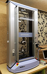
Precision tensile testing machine
Model
AUTO GRAPH AG-X plus (Made in Shimadzu plant)
Load capacity
50kN
Measurement accuracy
50kN±0.25kN
Microscopic strain area can be measured by a high-precision strain gauge.
By employing a particular method, the characteristic value of material for CAE can be analyzed with high precision.
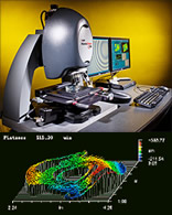
3D Optical Surface Profiler (ZYGO)
Model
New View7000
Minimum optical resolution
0.1nm
Non-contact type surface roughness/contour measuring instrument.
Zygo's patented scaning white-light technology (SWLI) and frequency domain (FDA) provides its vertical resolution to 0.1mm.
Improving a high image quality of optical system and speeding up data acquisition enables to measure surface shape faithfully.
Precision metal workpieces are measured with no contact.
Data is analyzable of stereoscopic display and 3D image analysis.
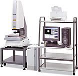
CNC Video Measuring System (Nikon: Nexiv)
Model
NEXIV VMR-1515 (Nikon)
Minimum display unit
0.1μm
Measurement accuracy
Z axes1.5+L/150μm
Measuring object
Package, substrate, stamping products, etc.
This automatically measures dimensions and configurations of various precision devices and electronic components with high accuracy by applying optical measuring technology and image processing technology.
Program detects an edges of the inspection object from captured images by CCD. It is enabled to measure complex surface shapes by processing data appropriately.
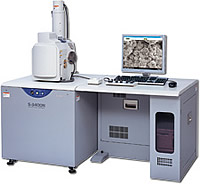
Scanning Electron Microscope (SEM)
Model
S-3400N (Hitachi)
Magnification
5x - 300,000x
Maximum sample size
φ200mm×80mm(H)
Applicable in various fields of R&D and inspection.
Resolution: 3.0nm ( high vacuum mode), 4.0nm (VP-mode)
Resolution: 135eV
Analyzing range: 10mm2
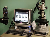
High-speed Microscope
Model
VW-9000 (KEYENCE)
High speed camera and microscope are equipped.
+ drop test, strength test, etc.
+ Press machine behavior
+ welding penetration
+ flow simulations of melted metal
+ observation of machining process etc.
This is the best used for for magnified observation and high-speed video recording at any sites.